- Published on
Teach My Girlfriend GPU 3: Deploy to Hardware
- Authors

- Name
- Yue Zhang
- Unified Shader Architecture: One Pool to Rule Them All
- GPU vs CPU: Redefining the "Core"
- SMs and Streaming Processors
- SIMD Width
- Hiding Memory Latency with Warp Scheduling
- Latency vs. throughput
- Cache and power consumption
This is the third episode of "Teach My Girlfriend GPUs." In the past two episodes, we covered the essential functions a modern GPU should logically include. Of course, when implementing those directly in hardware, you inevitably run into a lot of issues cost, performance, power consumption, and so on. Let’s now explore how those problems are solved.
Unified Shader Architecture: One Pool to Rule Them All
In early programmable GPUs like the GeForce FX5600 (2003), the pipeline was split: two vertex shader units and four pixel shader units. That design was most efficient when the vertex-to-pixel workload ratio was 1:2. But in real applications, triangle sizes and rendering loads vary. Sometimes there are many tiny triangles (more vertex work), and other times a single large one (more pixel work). These disparities lead to hardware underutilization — some units overloaded, others idle.
With increasingly complex pipelines, trying to hardwire every stage inevitably leads to load imbalance.
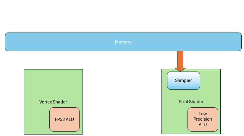
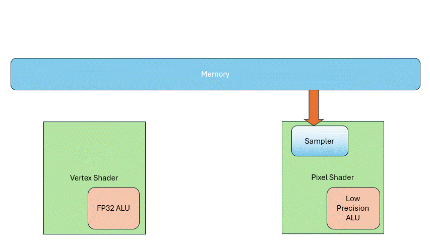
Before 2005, people thought Vertex Shaders needed 32-bit float precision for accurate coordinates, but they didn’t need texture sampling. Pixel Shaders, in contrast, mostly dealt with colors and base values—so high precision wasn’t necessary, but texture sampling was. This led to separate hardware units for each.
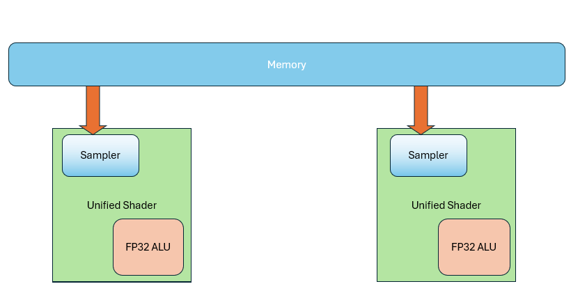
But as demand evolved, those boundaries blurred: Vertex Shaders started needing texture sampling for terrain rendering, and Pixel Shaders began doing general-purpose computations, so they too needed 32-bit float precision. The result: both units ended up with similar texture samplers and ALUs. Though they got more complex, they also became more uniform.
Then people discovered a solution that addressed both issues: shared execution units. This led to the Unified Shader Architecture. Now the same hardware executes all shader types— no more fixed units just for vertex or pixel shaders.
NOTE
In the pipeline, those stages still exist logically,but they use shared hardware.
So how do you know when to run vertex vs. pixel shaders? That’s where a scheduler comes in. If you need X vertex shaders and Y pixel shaders, the scheduler dynamically allocates the shared hardware accordingly. This solves load imbalance dynamically, and simplifies hardware design.
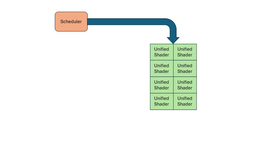
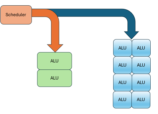
The same principle applies to other functional units. For example, texture sampling is usually less frequent than computation, so you can have fewer samplers than ALUs, and let the scheduler manage the sharing.
Other fixed-function units can also be scheduled this way. Take the GeForce RTX 3090 Ti, for instance: It has 10,752 unified shader cores, 336 samplers, and 112 raster and pixel operation units. Despite having many shader types, the hardware execution units are the same.
GPU vs CPU: Redefining the "Core"
Why do GPUs have tens of thousands of "cores" while CPUs consider a few dozen impressive? It’s mainly because the definition of a "core" is different.
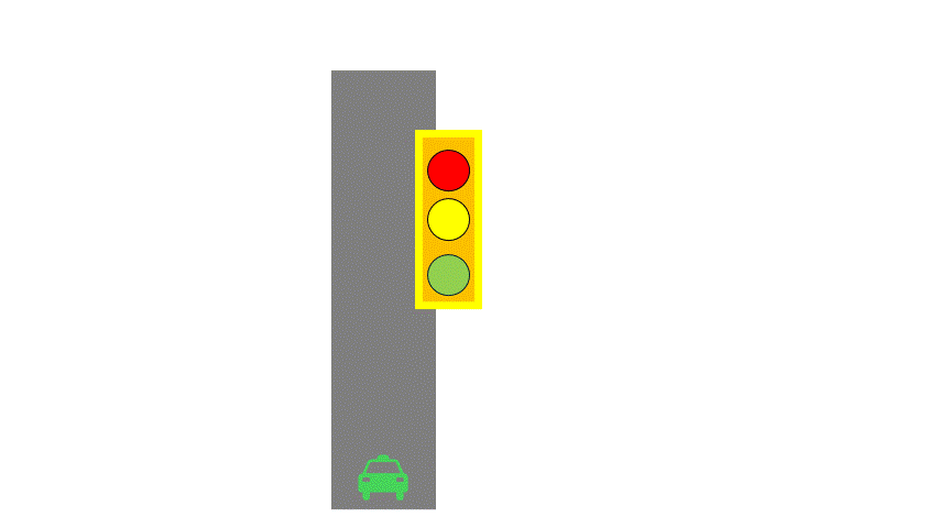
Let’s introduce two computer architecture concepts: SISD (Single Instruction Single Data) and SIMD (Single Instruction Multiple Data). To make this easier, imagine a highway analogy:
- Instructions are like traffic lights,
- Data is like cars,
- Data streams are like road lanes.
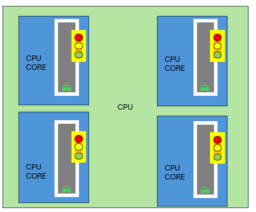
In SISD, you have a single-lane road with one traffic light controlling traffic.
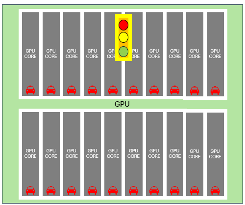
In SIMD, multiple lanes share the same light— all lanes must follow the same direction.

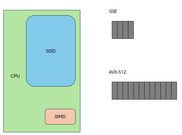
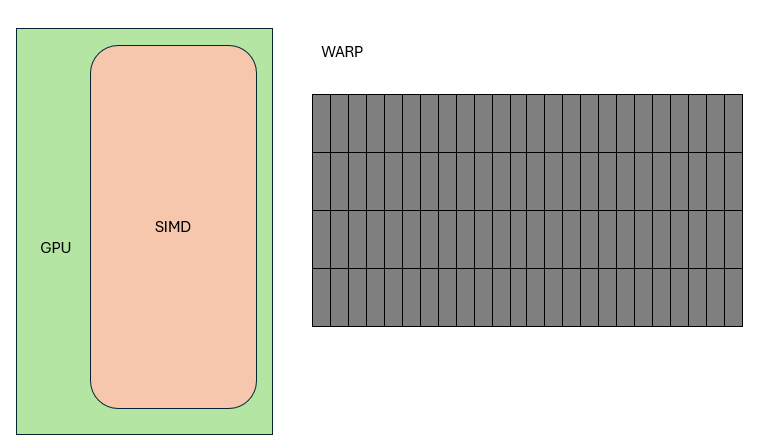
A CPU core is like SISD, supplemented by SIMD instruction sets, like SSE, which can process four numbers at once, like four-lane roads. AVX512 now supports 16-wide lanes. Logically, all these threads execute the same instruction at the same time. This group of threads is called a Warp (NVIDIA) or Wave (AMD).
In contrast, a "core" in GPU terminology refers to a single lane in SIMD, and GPU SIMD widths are large: 16, 32, 64, even 128.
So:
- CPU core count = number of roads.
- GPU core count = number of lanes.
They aren’t equivalent. To compare directly, you’d have to multiply CPU cores by the SIMD width (e.g., 4 for SSE), or divide GPU cores by warp width (e.g., 32).
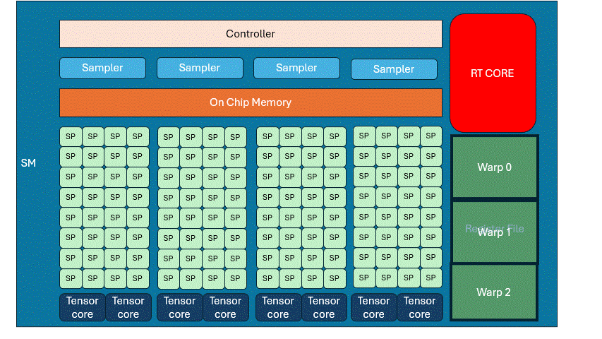
SMs and Streaming Processors
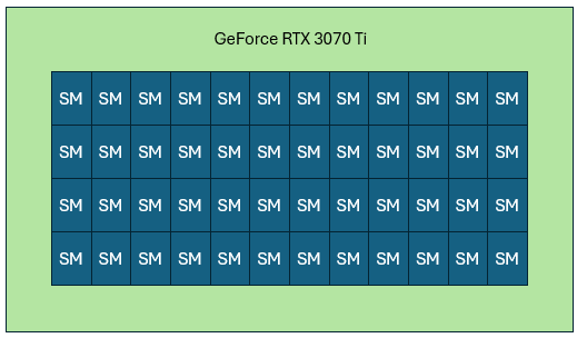
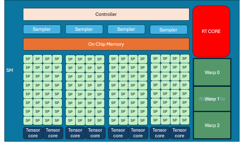
A GPU "core" is actually a Streaming Processor (SP). A group of SPs + control logic + local memory makes up a Streaming Multiprocessor (SM). For example, in NVIDIA RTX 30 series: Each SM has 128 SPs and 4 samplers.
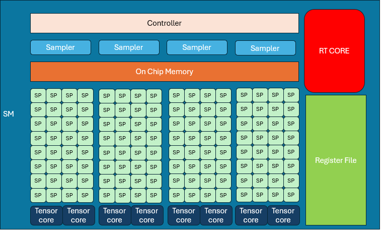
SMs are the GPU’s primary building blocks. 3070Ti has 48 SMs, each SM is structurally identical.
SIMD Width
GPU SIMD is wide. Most transistors go toward computation, a few toward control. Like a traffic light controlling 32 lanes—if one stops, they all stop. If one goes, they all go.
But this approach has downsides.
If you only have 2–3 cars on a 32-lane road, you’re wasting hardware. Software must fill all lanes with tasks.
Second: all 32 lanes must execute the same instruction. Either all going straight of all turning left. But what if some of the 32 cars want to go sztraight and some want to turn left?
That’s branch divergence. To maintain SIMD behavior, both branches must run— then use a select() operation to pick the right result. This wastes computation and increases power consumption.
Hiding Memory Latency with Warp Scheduling
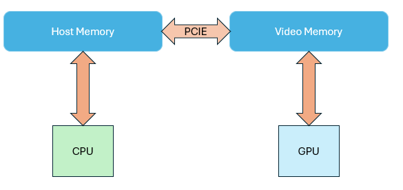
Wide computation needs fast memory access. Discrete GPUs have dedicated memory: VRAM, while CPU uses main memory. VRAM is usually GDDR, with bus widths from 128–512 bits—much wider than DDR (32–64 bits).
It's designed to trade high latency for high throughput. Latency is much higher than host memory.
NOTE
It means when you want to read the data of the VRAM, it has to wait until a batch before returning back to you
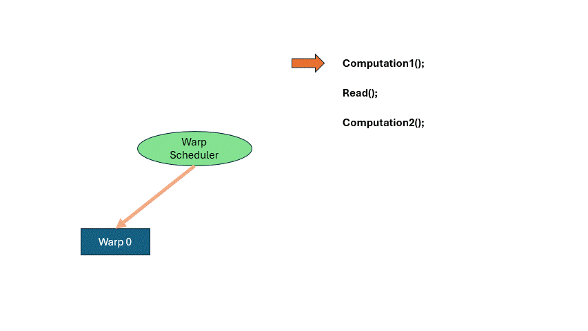
If you wait idly for memory, GPU efficiency crashes. Let’s say a program does some computation, loads memory, and then computes again. When a Warp reaches READ, it has to wait. That’s where the Warp Scheduler comes in. It pauses the current warp, activates another. Repeat this cycle until the first warp finishes memory access. This is called hiding memory latency with computation. It lets the GPU run far more threads than it has cores.
There is a register space inside the SM, each warp occupies a part fot local variables, etc. If the entire space is fully occupied, there is no way to schedule more warps to come in, and you have to really stop and wait for the memory to be read.
This is the case where memory latency cannot be hidden by computation, which will reduce the efficiency. To optimize it, it needs to modify the algorithm or data size to reduce the memory occupation.
Latency vs. throughput
- CPU = low latency,
- GPU = high throughput.
Think of CPU as a car, quick to start, few passengers. GPU is a bus, slow to load, but carries many people per trip.
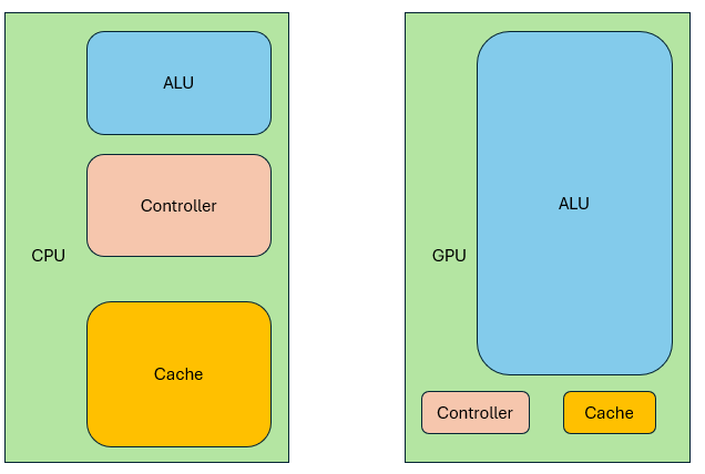
Cache and power consumption
Because GPUs can hide memory latency, they don’t need big caches. CPUs, in contrast, require large multi-level caches to reduce latency. But caches consume a lot of power. So GPUs save power by using warp scheduling instead of large caches.