- Published on
In-Depth GPU Hardware Architecture and Operating Mechanisms
- Authors

- Name
- Yue Zhang
- Overview of GPU Rendering
- GPU Logical Pipeline
- GPU Key Technical Points
- GPU Resource Mechanisms
- Shader Execution Mechanism
Overview of GPU Rendering
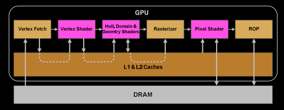
 Starting with the Fermi architecture, NVIDIA has adopted a similar principle in its designs. A Giga Thread Engine is used to manage all ongoing tasks. The GPU is divided into multiple GPCs (Graphics Processing Clusters), each containing several SMs (Streaming Multiprocessors, also called SMX or SMM) and a Raster Engine. These components are interconnected, most notably through a Crossbar, which links GPCs to other functional modules (such as ROPs or other subsystems).
Programmers write shaders, which are executed on the SMs. Each SM contains numerous cores designed to perform mathematical operations for threads. For example, a thread could represent a vertex or pixel shader invocation. These cores, along with other units, are driven by the Warp Scheduler, which manages a group of 32 threads as a Warp and dispatches instructions to the Dispatch Units.
The actual number of these units (e.g., how many SMs per GPC, how many GPCs, etc.) depends on the specific chip configuration. For instance, the GM204 (Maxwell architecture) has 4 GPCs, each with 4 SMs, while the Tegra X1 (also Maxwell-based) has 1 GPC and 2 SMs. The design of the SM itself (e.g., number of cores, instruction units, schedulers) has evolved over time, contributing to the GPU's efficiency and scalability, enabling it to power devices ranging from high-end desktops to mobile laptops.
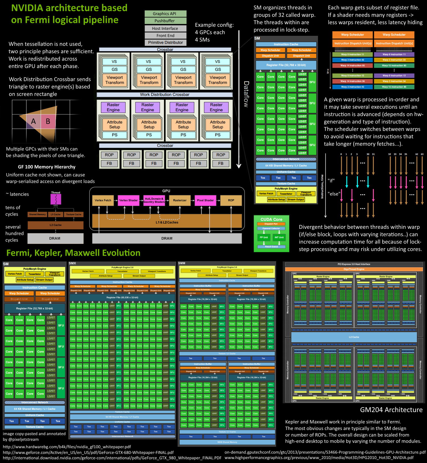
 As shown in the diagram, for certain GPUs (such as some Fermi models), a single SM (Streaming Multiprocessor) includes the following components:
- 32 Cores (Stream Processors): Primary computation units for executing mathematical operations.
- 16 LD/ST (Load/Store) Units: Handle data loading and storing operations.
- 4 SFUs (Special Function Units): Execute special mathematical functions like
sin,cos, andlog. - 128KB Register File: High-speed memory for storing data for active threads.
- 64KB L1 Cache: Fast cache memory to reduce data access latency.
- Global Memory Cache (Uniform Cache): Provides cached access to global memory.
- Texture Fetch Units: Specialized units for reading texture data.
- Texture Cache: Dedicated cache for storing texture data for faster access.
- PolyMorph Engine: Handles attribute setup, vertex fetching, tessellation, and rasterization (specialized for vertex-related tasks).
- 2 Warp Schedulers: Manage warp scheduling, where a warp consists of 32 threads. Instructions are dispatched to cores via Dispatch Units.
- Instruction Cache: Stores frequently used instructions for quick access.
- Interconnect Network: Internal network for communication between components.
GPU Logical Pipeline
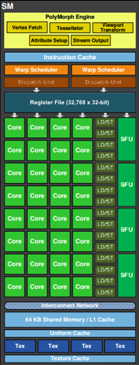
The application uses a graphics API (such as DirectX, OpenGL, or WebGL) to issue drawcall commands. These commands are sent to the GPU driver, which checks their validity. Valid commands are placed in a Pushbuffer, a memory region accessible by the GPU.
After a certain period or upon an explicit flush call, the driver sends the contents of the Pushbuffer to the GPU.The GPU receives these commands through the Host Interface. The Front End of the GPU processes these commands, preparing them for further stages.
- The Primitive Distributor takes over, processing the vertex data from the index buffer and generating triangles.These triangles are grouped into batches and distributed across multiple GPCs (Graphics Processing Clusters). For example, if
ntriangles are submitted, they are divided and assigned to several GPCs for parallel processing.
In the GPC (Graphics Processing Cluster), the PolyMorph Engine within each SM fetches vertex data using triangle indices. This is handled by the Vertex Fetch module, which retrieves the necessary data for processing.
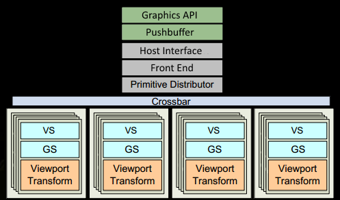
After fetching vertex data, it is processed by warps, which are groups of 32 threads. Warps follow the SIMT (Single Instruction, Multiple Threads) model, where all 32 threads execute the same instruction simultaneously but on different data. This approach allows for efficient decoding and execution, making the chip smaller and faster.
The Warp Scheduler in the SM dispatches instructions to the entire warp in order. Threads within a warp execute in lock-step, meaning they run the same instruction at the same time. If a thread encounters an inactive condition (e.g.,
if(false)), it is masked out but still consumes a clock cycle. Branching in shaders (e.g.,if-else, loops) can significantly increase execution time because all branches are executed unless all 32 threads in a warp follow the same path.IMPORTANT
Threads cannot execute instructions independently; they operate in warps, Warps are the smallest unit of execution in the GPU, and warps themselves are independent of each other.
Instructions in a warp may complete in one cycle or require multiple cycles, depending on the operation. For example, LD/ST (Load/Store) units are fewer in number compared to basic math units, causing potential bottlenecks.
Some instructions, such as memory loads, take longer to complete than others. To address this, the Warp Scheduler switches to another warp that is not waiting for memory. This is a key mechanism GPUs use to overcome memory latency: by simply switching between active thread groups. To make this switching extremely fast, each warp managed by the scheduler has its own set of registers in the Register File. A conflict arises here: the more registers a shader requires, the less registers is available for warps. This results in fewer active warps. When memory latency occurs, there may be no other warps available to switch to, leading to idle waiting.
- Once a warp completes all instructions in the vertex shader, the results are processed by the Viewport Transform module. Triangles are clipped and prepared for rasterization.
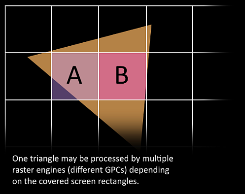
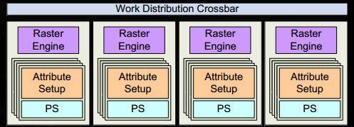
- Then, the triangles are divided and assigned to multiple GPCs. The range of each triangle determines which raster engine it will be assigned to. Each raster engine covers multiple tiles on the screen. This means the rendering of a triangle is distributed across multiple tiles. At this stage, the rendering process shifts from being triangle-based to pixel-based, as the triangles are now processed according to the displayed pixels within each tile.
The Attribute Setup in the SM ensures that data from the vertex shader is interpolated and made readable for the pixel shader.
The raster engines in the GPC work on the received triangles, generating pixel information for these triangles. They also handle clipping, backface culling, and Early-Z culling.
32 pixel threads are grouped together, or equivalently, 8 blocks of 2x2 pixels, which is the smallest working unit in the pixel shader. If a pixel thread is not covered by a triangle, it is masked out. The Warp Scheduler in the SM manages the tasks of the pixel shader.
The subsequent stages follow the same logical steps as in the vertex shader, but are executed within the pixel shader threads. Since fetching values within a pixel incurs no performance cost, lock-step execution is highly efficient. All threads are guaranteed to execute instructions at the same point.
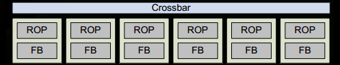
- Once the pixel shader has completed calculating the color and depth values, the data must respect the original API order of the triangles before being handed over to the ROP (Render Output Unit). An ROP contains multiple ROP units, which handle depth testing and framebuffer blending. Depth and color updates must be performed as atomic operations to avoid conflicts or errors when two different triangles affect the same pixel.
GPU Key Technical Points
The previous section focused on the internal workflow and mechanisms of the GPU. For simplicity, many details and processes were omitted. This section will provide further explanations and clarifications.
SIMD and SIMT
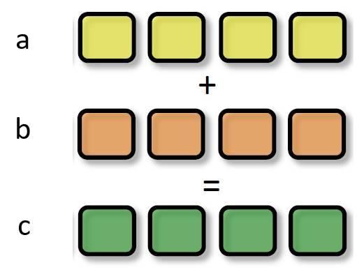
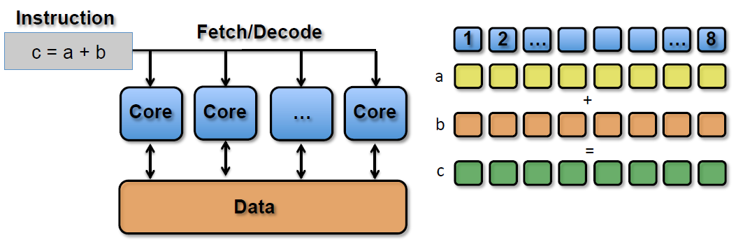
SIMD refers to executing a single instruction on multiple data points simultaneously. In the GPU's ALU (Arithmetic Logic Unit), a single instruction can process multi-dimensional vector data (typically 4D).
float4 c = a + b; // a and b are of type float4
On a processing unit without SIMD, this operation would require 4 separate instructions to add the four float values. The assembly pseudocode would look like this:
ADD c.x, a.x, b.x
ADD c.y, a.y, b.y
ADD c.z, a.z, b.z
ADD c.w, a.w, b.w
With SIMD technology, the same operation can be completed in a single instruction:
SIMD_ADD c, a, b
SIMT (Single Instruction, Multiple Threads) is an advanced version of SIMD, designed to handle parallel processing in GPUs more flexibly. In SIMT, a single instruction is executed simultaneously across multiple threads within a single SM (Streaming Multiprocessor). Each Core in the SM processes the same instruction but operates on different data.
SIMT_ADD c, a, b
Handling if-else Statements in SIMT
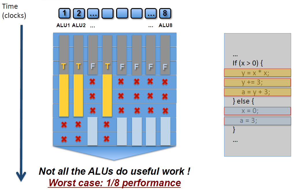 As shown in the diagram, an SM contains 8 ALUs (Cores). Due to the SIMD (Single Instruction, Multiple Data) nature, each ALU processes different data. This causes the
 if-else statement to execute the true branch (yellow) on some ALUs and the false branch (blue-gray) on others.Result: Many ALUs are masked out and their execution cycles are wasted, which increases the overall execution time. Worst-case Scenario: Only 1/8 of the SM's ALUs are utilized (where 8 is the number of threads in the SM; this number may vary depending on the GPU architecture).
Similar to if-else statements, for loops can also cause performance inefficiencies in GPU programming due to warp divergence. Consider the following shader code:
void func(int count, int breakNum) {
    for (int i = 0; i < count; ++i) {
        if (i == breakNum)
            break;
        else
            // do something
    }
}
Since each ALU (Core) has a different value for count and may encounter the break statement at different times, the fastest ALU might finish executing the shader in 1/N of the time compared to the slowest ALU.
- However, due to the SIMD (Single Instruction, Multiple Data) nature of the GPU, the fastest ALU must wait for the slowest ALU to finish before proceeding to the next set of instructions.
- This results in wasted execution cycles and reduced overall efficiency.
Early-Z
Pixel Quad
In Step 13 from the Previous Section
32 pixel threads are grouped together, or equivalently, 8 blocks of 2x2 pixels, which is the smallest working unit in the pixel shader. If a pixel thread is not covered by a triangle, it is masked out. The Warp Scheduler in the SM manages the tasks of the pixel shader.
In the pixel shader, adjacent 4 pixels are grouped together as an inseparable unit and sent to 4 different Cores within the same SM. But why is the smallest processing unit a 2x2 pixel block?
Here are some possible reasons:
Grouping pixels into 2x2 blocks simplifies the process of assigning work to Cores, reducing overhead and improving efficiency.
This design reduces the number and size of hardware units required in the SM, making the architecture more compact and efficient.
Processing pixels in groups allows for better utilization of resources, lowering power consumption and increasing performance per watt.
Even if some pixels in the 2x2 block are invalid (not covered by a triangle), they can still assist in calculating derivatives (e.g., for texture filtering) for the valid pixels. This is further explained later.
GPU Resource Mechanisms
This section explains the mechanisms of memory access and resource management in GPUs.
Memory Architecture
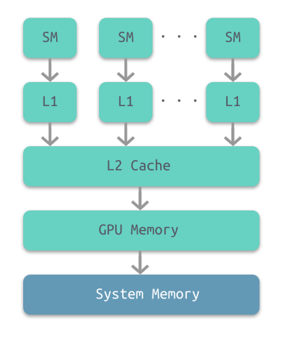 The access speed of memory types in GPUs decreases progressively from registers to system memory:
| Memory Type | Registers | Shared Memory | L1 Cache | L2 Cache | Texture/Constant Cache | Global Memory |
|---|---|---|---|---|---|---|
| Access Latency (Cycles) | 1 | 1~32 | 1~32 | 32~64 | 400~600 | 400~600 |
The multi-level cache structure described above is often referred to as "CPU-Style" memory architecture. However, GPUs also employ a "GPU-Style" memory architecture.
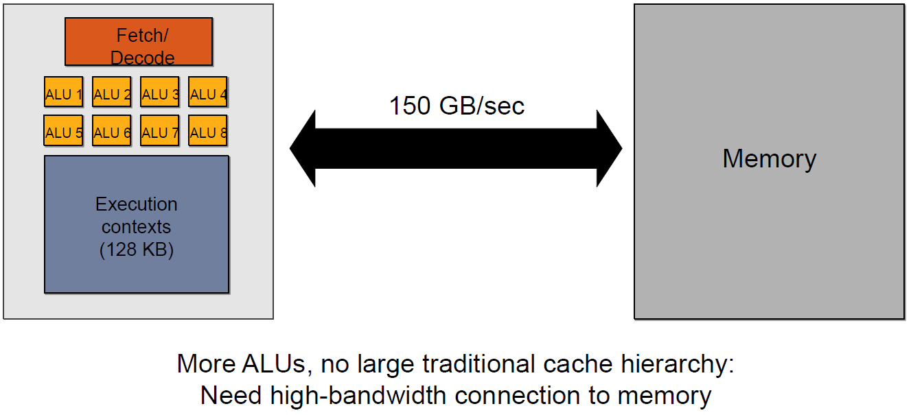 The GPU-Style memory architecture is characterized by the following features: High Number of ALUs, Multiple GPU Contexts, High Throughput, High Bandwidth Memory Access
GPU Context
CAUTION
Context below can be viewed as one Warp
Different warps within the same SM can execute different instructions.
Consider an SM running two warps: The SM can execute instructions from Warp A and Warp B simultaneously, as long as there are enough execution units available.
- Warp A: Executing a vertex shader.
- Warp B: Executing a fragment shader.
The SIMT (Single Instruction, Multiple Threads) model used in modern GPUs introduces certain limitations on the independence of cores within an SM (Streaming Multiprocessor). When cores access high-latency memory (e.g., textures, constant cache, global memory), it can lead to significant stalls, reducing overall performance.
For example, in the diagram below, there are four warps (Contexts) that share the same set of ALU (Arithmetic Logic Units).
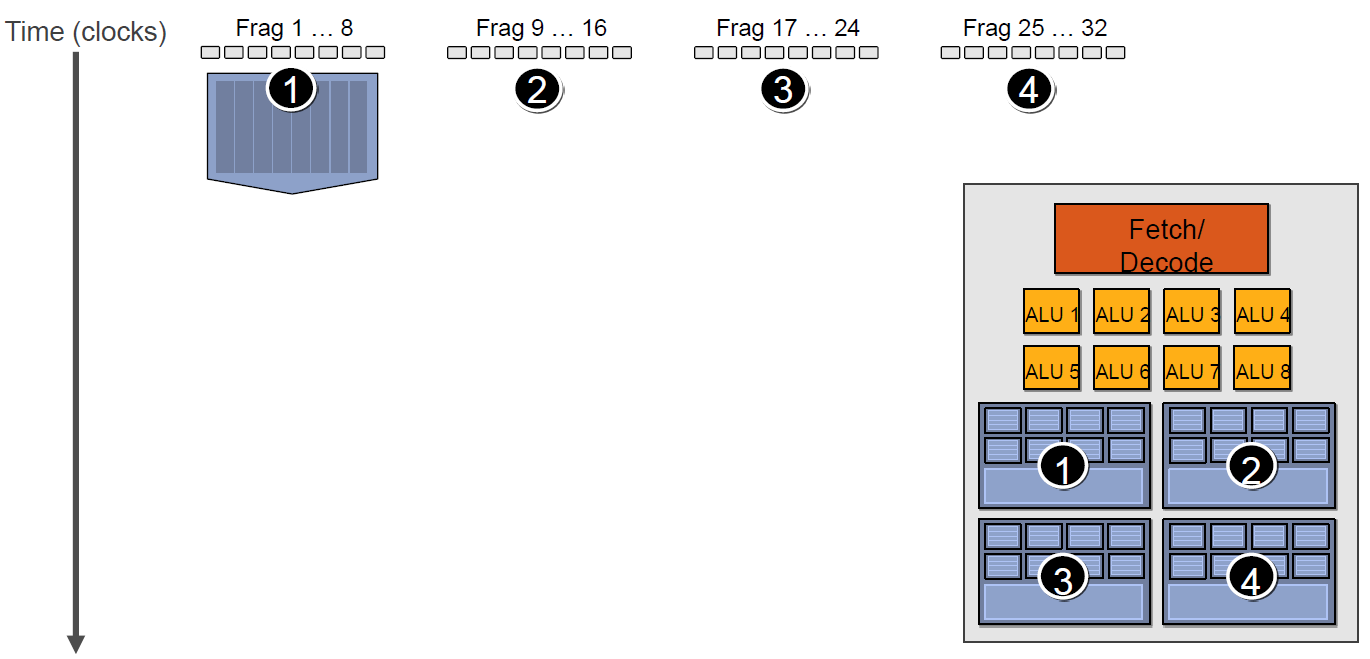 If the first Context needs to access the cache or memory, it will incur a 2-3 cycle delay. During this time, the scheduler will activate the second Context to utilize the ALU efficiently.
 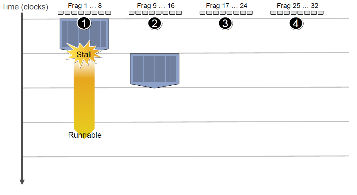 If the second Context also gets stalled while accessing the cache or memory, the scheduler will sequentially activate the third and fourth Contexts. This process continues until either the **first
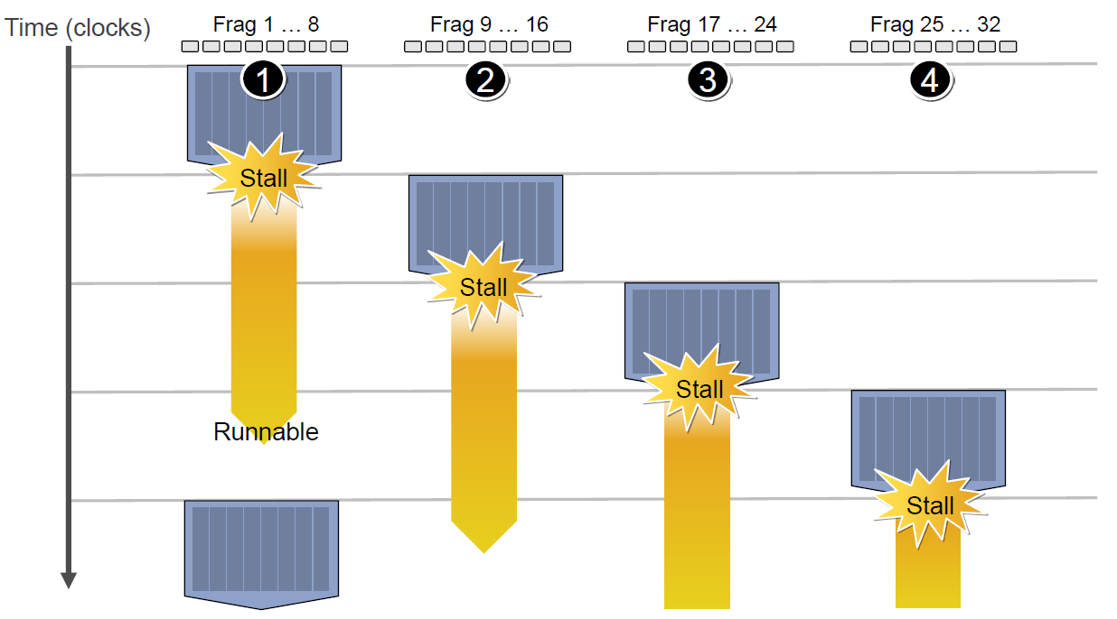 As a consequence of the delay, the overall execution time for each Context is extended.
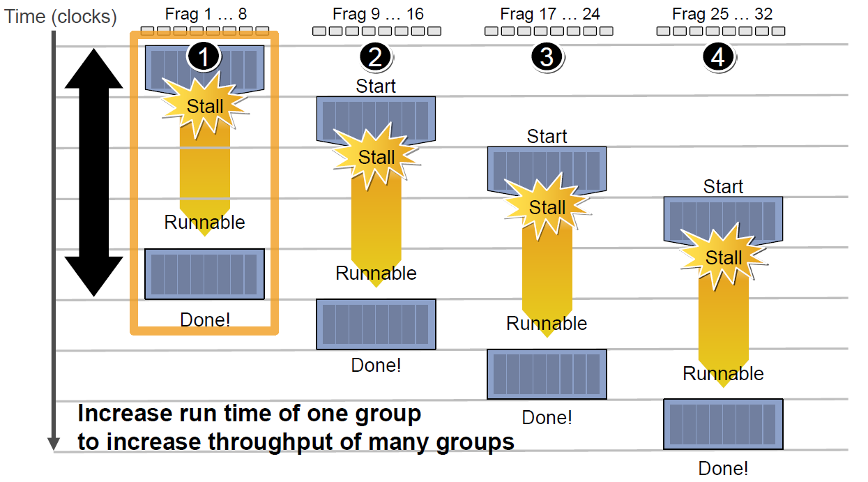 However, having more available Contexts improves the throughput of the compute units. For example, in the diagram below, an architecture with 18 Contexts can maximize throughput.
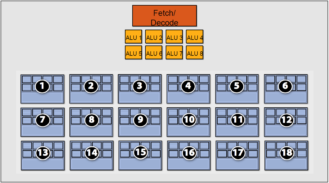
In Vulkan, there is no single "context" in the traditional OpenGL sense. Instead, Vulkan uses explicit objects (e.g., command buffers, descriptor sets, pipelines) and explicit state management to achieve similar functionality. Switching between different "contexts" (e.g., rendering setups) involves manually reconfiguring these objects. Below is a guide to switching between different rendering configurations in Vulkan:
Vulkan eliminates the concept of a global context (like OpenGL’s stateful model) in favor of an explicit, object-based design. Developers must define and manage all resources, state, and dependencies explicitly, removing hidden driver-managed state. Here’s how Vulkan achieves this:
Key Differences Between Vulkan and OpenGL
| Feature | OpenGL | Vulkan |
|---|---|---|
| State Management | Implicit global state (e.g., glBindTexture, glUseProgram). | Explicit, object-based state (e.g., pipelines, descriptor sets). |
| Resource Binding | Global bind points (e.g., texture unit 0). | Explicit descriptor sets and resource bindings. |
| Command Execution | Immediate-mode rendering (commands execute immediately). | Deferred command buffers (commands recorded ahead of time). |
| Driver Overhead | High (driver manages state validation). | Low (developer handles validation upfront). |
| Thread Safety | Single-threaded (global context per thread). | Multi-threaded (command buffers can be recorded in parallel). |
How Vulkan Works Without a Global Context
Explicit Object-Based Design
- Pipelines: Vulkan uses VkPipeline objects to encapsulate all rendering state (shaders, blending, depth testing, etc.). No hidden state: You must bind a pipeline explicitly before rendering.
- Descriptor Sets: Resources (textures, buffers) are bound via VkDescriptorSet objects. No global texture units: You explicitly bind descriptor sets to shaders.
Command Buffers: Commands are recorded into VkCommandBuffer objects ahead of time. No immediate execution: Commands are batched and submitted to queues later.
Explicit Resource Management
- Memory Allocation: You allocate GPU memory explicitly using VkDeviceMemory and bind it to resources (buffers/textures).
- Synchronization: You manage synchronization explicitly with semaphores (VkSemaphore) and fences (VkFence).
No Global State
Thread Safety: Command buffers can be recorded in parallel across threads (no global context).
No Hidden State: Every operation (e.g., binding a texture) must be explicitly specified in the command buffer.
GPU Resource Management Model
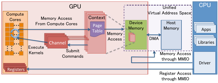
MMIO (Memory Mapped IO)
- CPU and GPU communicate through MMIO.
- CPU accesses GPU register states via MMIO.
- DMA transfers large amounts of data using MMIO for command control.
- I/O ports can be used for indirect MMIO access, but open-source software like Nouveau never accesses them.
1.GPU Context
- Represents the state of GPU computation.
- Each GPU context has its own virtual address space.
- Multiple active contexts can exist simultaneously within a GPU.
GPU Channel
- All commands are issued by the CPU.
- Commands are submitted as a command stream to a hardware unit called GPU Channel.
- Each GPU Channel is associated with a GPU Context, and a single GPU Context can have multiple GPU Channels.
- Each GPU Context contains GPU Channel Descriptors, which are objects stored in GPU memory.
- Each GPU Channel Descriptor stores channel settings, including the Page Table.
- Each GPU Channel has a dedicated command buffer in GPU memory, which is visible to the CPU via MMIO.
- GPU Context Switching and command execution are scheduled internally by GPU hardware.
GPU Page Table
- GPU Contexts are isolated from each other via Page Tables.
- GPU Page Tables are separate from CPU Page Tables and reside in GPU memory.
- The physical address of a GPU Page Table is stored in the GPU Channel Descriptor.
- GPU Page Tables not only map GPU virtual addresses to GPU physical memory but can also map to CPU physical addresses.
- This enables a unified virtual address space for both GPU and CPU.
PCI-e BAR
- The GPU connects to the host system via the PCI-e bus.
- Base Address Registers (BARs) provide MMIO windows configured at GPU startup.
- GPU control registers and memory are mapped into BARs.
- GPU device memory is accessed through the mapped MMIO windows.
PFIFO Engine
- PFIFO is a special unit that handles GPU command submission.
- Maintains independent command queues (Channels).
- These command queues operate as Ring Buffers with PUT and GET pointers.
- PFIFO intercepts all execution instructions that access the Channel control area.
- The GPU driver uses Channel Descriptors to store related Channel settings.
- PFIFO forwards commands to the PGRAPH Engine for execution.
BO (Buffer Object)
- A Buffer Object (BO) is a memory block used to store: Textures Render Targets Shader code And more GPU-related data.
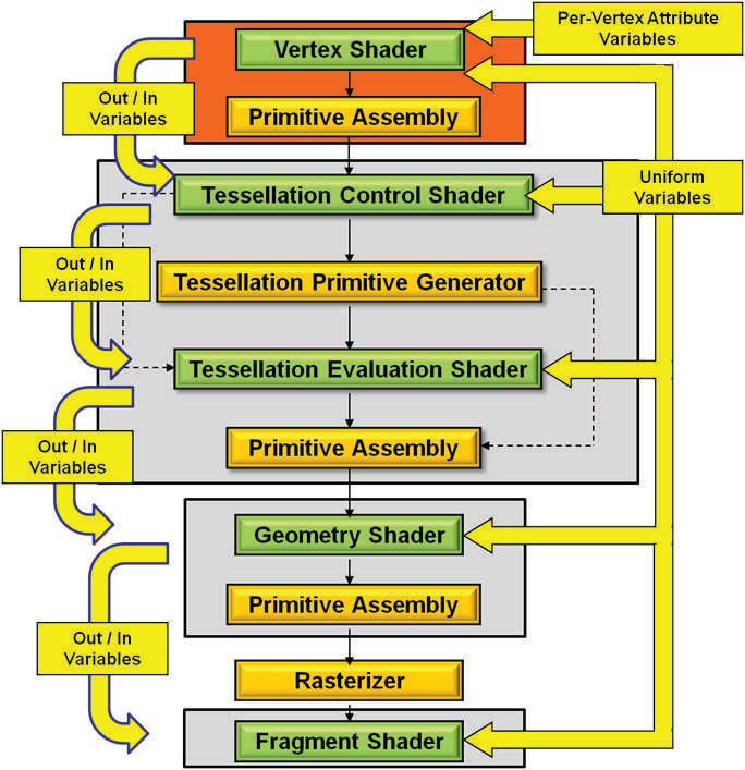
Shader Execution Mechanism
Shader code, like traditional programming languages (e.g., C++), follows a compilation process to transform human-readable high-level code into machine-executable binary instructions
The process of compiling high-level language code into assembly instructions is typically performed offline to reduce runtime overhead.
During the execution phase, the CPU sends shader binary instructions to the GPU via PCI-e. When executing the code, the GPU uses Context to divide the instructions into multiple Channels, which are then pushed to the storage space of different Cores.
For modern GPUs, the number of programmable stages has increased, including but not limited to:
- Vertex Shader
- Tessellation Control Shader
- Geometry Shader
- Fragment (Pixel) Shader
- Compute Shader
- ...
Extension
// 开启扩展
#extension GL_NV_shader_thread_group : require     (or enable)

WARP_SIZE_NV	// 单个线程束的线程数量
WARPS_PER_SM_NV	// 单个SM的线程束数量
SM_COUNT_NV		// SM数量

uniform uint  gl_WarpSizeNV;	// 单个线程束的线程数量
uniform uint  gl_WarpsPerSMNV;	// 单个SM的线程束数量
uniform uint  gl_SMCountNV;		// SM数量

in uint  gl_WarpIDNV;		// 当前线程束id
in uint  gl_SMIDNV;			// 当前线程束所在的SM id,取值[0, gl_SMCountNV-1]
in uint  gl_ThreadInWarpNV;	// 当前线程id,取值[0, gl_WarpSizeNV-1]

in uint  gl_ThreadEqMaskNV;	// 是否等于当前线程id的位域掩码。
in uint  gl_ThreadGeMaskNV;	// 是否大于等于当前线程id的位域掩码。
in uint  gl_ThreadGtMaskNV;	// 是否大于当前线程id的位域掩码。
in uint  gl_ThreadLeMaskNV;	// 是否小于等于当前线程id的位域掩码。
in uint  gl_ThreadLtMaskNV;	// 是否小于当前线程id的位域掩码。

in bool  gl_HelperThreadNV;	// 当前线程是否协助型线程。
The variable gl_HelperThreadNV specifies if the current thread is a helper thread. In implementations supporting this extension, fragment shader invocations may be arranged in SIMD thread groups of 2x2 fragments called "quad". When a fragment shader instruction is executed on a quad, it's possible that some fragments within the quad will execute the instruction even if they are not covered by the primitive. Those threads are called helper threads. Their outputs will be discarded and they will not execute global store functions, but the intermediate values they compute can still be used by thread group sharing functions or by fragment derivative functions like dFdx and dFdy.
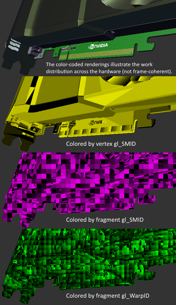 By utilizing NV extension fields, we can visualize the SM and Warp IDs in vertex shaders and pixel shaders. This provides insights into the GPU's execution mechanism and workflow, allowing us to better understand its operation.
First, in the application, create vertex data that includes two triangles.
// set up vertex data (and buffer(s)) and configure vertex attributes
const float HalfSize = 1.0f;
float vertices[] = {
	-HalfSize, -HalfSize, 0.0f, // left bottom
	HalfSize, -HalfSize, 0.0f,  // right bottom
	-HalfSize,  HalfSize, 0.0f, // top left

	-HalfSize,  HalfSize, 0.0f, // top left
	HalfSize, -HalfSize, 0.0f,  // right bottom
	HalfSize,  HalfSize, 0.0f,  // top right
};
Vertex Shader:
#version 430 core

layout (location = 0) in vec3 aPos;

void main()
{
	gl_Position = vec4(aPos, 1.0f);
}
Fragment Shader:
#version 430 core
#extension GL_NV_shader_thread_group : require

uniform uint  gl_WarpSizeNV;	// 单个线程束的线程数量
uniform uint  gl_WarpsPerSMNV;	// 单个SM的线程束数量
uniform uint  gl_SMCountNV;		// SM数量

in uint  gl_WarpIDNV;		// 当前线程束id
in uint  gl_SMIDNV;			// 当前线程所在的SM id,取值[0, gl_SMCountNV-1]
in uint  gl_ThreadInWarpNV;	// 当前线程id,取值[0, gl_WarpSizeNV-1]

out vec4 FragColor;

void main()
{
	// SM id
	float lightness = gl_SMIDNV / gl_SMCountNV;
	FragColor = vec4(lightness);
}
 From the analysis above, we can gather the following insights:
- The image consists of 32 brightness levels, indicating that the GeForce RTX 2060 has 32 SMs (Streaming Multiprocessors).
- Each SM renders a 16x16 pixel block at a time, meaning each SM has 256 Cores.
- Pixel blocks are not assigned sequentially across SMs but are distributed in a non-uniform manner.
- Discontinuities appear at the junctions between different triangles, suggesting that if a single pixel block belongs to different triangles, it gets assigned to different SMs for processing.
- Based on this observation, we can infer that in a region of the same area, if it contains more triangles, the number of SM assignments increases, leading to higher rendering performance costs.
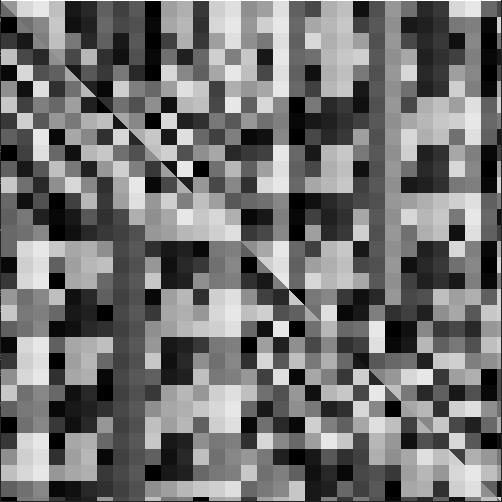
Next, modify the fragment shader color computation code to display the Warp ID.
// warp id
float lightness = gl_WarpIDNV / gl_WarpsPerSMNV;
FragColor = vec4(lightness);
 From this, we can derive the following insights and conclusions:
- The image consists of 32 brightness levels, indicating that each SM contains 32 Warps, and each Warp consists of 8 Cores.
- Each color block in the image represents a 4x8 pixel region.
- Since each Warp has 8 Cores, we can infer that each Core processes a 2x2 pixel block per cycle.
- Pixel blocks are assigned in a non-uniform manner, similar to the previous SM allocation pattern.
- Discontinuities appear at triangle edges, consistent with the earlier SM-level findings.
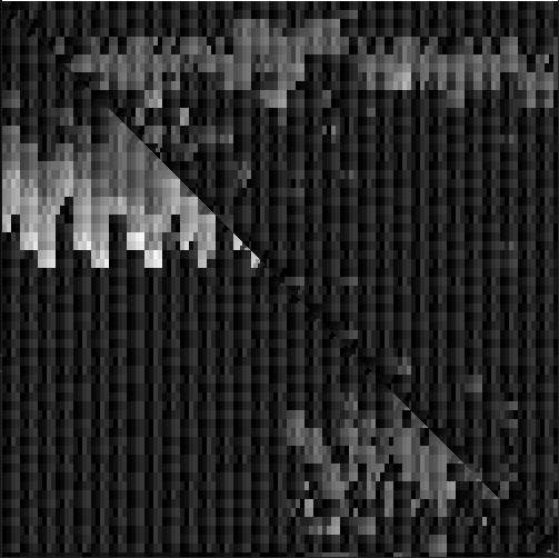
Next, modify the fragment shader color computation code to display the Thread ID.
// thread id
float lightness = gl_ThreadInWarpNV / gl_WarpSizeNV;
FragColor = vec4(lightness);
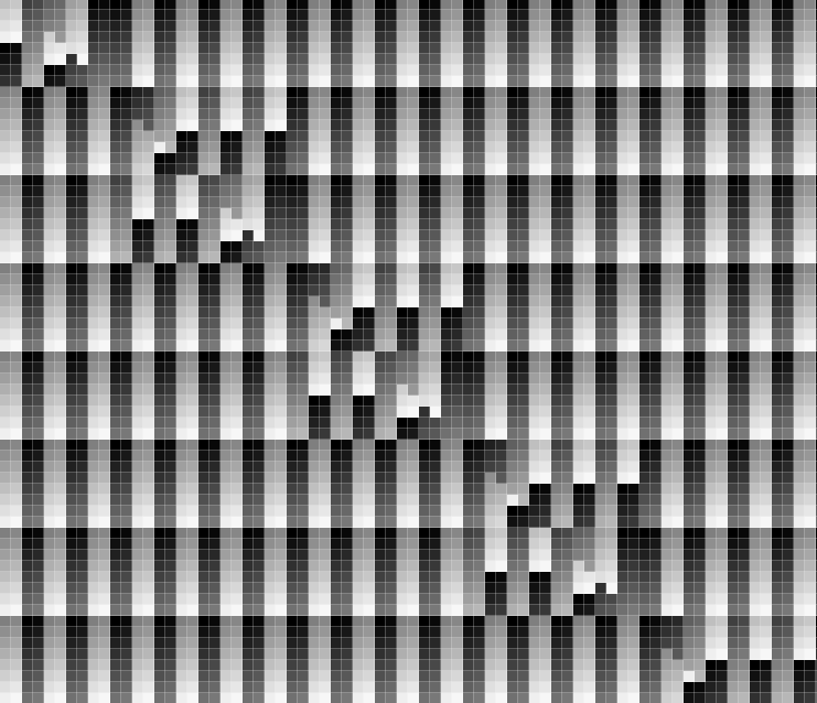 By analyzing the two previous images, we can draw the following conclusions:
- Compared to SM and Warp distribution, thread distribution is more regular, indicating that threads within the same Warp follow a structured layout.
- Disruptions appear at triangle boundaries, suggesting that different Warps handle different sets of threads.
- The image contains 32 brightness levels, confirming that a single Warp consists of 32 threads.
- Each pixel has a unique brightness level, differing from its neighboring pixels. This implies that each thread processes exactly one pixel.